PRODUCTS
LEGACY TELCO OSS & BSS PRODUCTS
SDI VIDEO OVERLAY PRODUCTS
IP CORE AND FPGA PRODUCTS
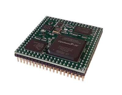
CONFIGURABLE PROCESSOR MODULES
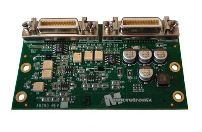
HSMC DAUGHTERCARDS
TECHNICAL SUPPORT CONTRACTS
APPLICATION EXAMPLES
Glitch-free 2x1 SDI Video Switching
Text Overlay with PIP Display
Alpha-blended Overlay of Computer-Generated Graphics
Scrolling RSS Newsfeed with Time, Date and Logo Overlay
Active GPS Text and Graphic Overlay
DESIGN SERVICES
VIDEO PROJECTS
OTHER CUSTOMER PROJECTS
RESOURCES
DOCUMENT LIBRARY
TELCO OSS & BSS DOCUMENTS
IP CORE AND FPGA DOCUMENTS
SDI VIDEO OVERLAY DOCUMENTS
SOFTWARE UPDATES
X.25 & SERIAL GATEWAY PRODUCTS
VIDEO PRODUCTS
IP CORE PRODUCTS
TECHNICAL SUPPORT
FAQs
RESELLERS
SDI VIDEO & IP PRODUCTS
TECHNOLOGY PARTNERS
CONTACT US
REQUEST A QUOTE
Search
Get in touch
sales@microtronix.com
PAY INVOICE
CART
0
PRODUCTS
LEGACY TELCO OSS & BSS PRODUCTS
SDI VIDEO OVERLAY PRODUCTS
IP CORE AND FPGA PRODUCTS
CONFIGURABLE PROCESSOR MODULES
HSMC DAUGHTERCARDS
TECHNICAL SUPPORT CONTRACTS
APPLICATION EXAMPLES
Glitch-free 2x1 SDI Video Switching
Text Overlay with PIP Display
Alpha-blended Overlay of Computer-Generated Graphics
Scrolling RSS Newsfeed with Time, Date and Logo Overlay
Active GPS Text and Graphic Overlay
DESIGN SERVICES
VIDEO PROJECTS
OTHER CUSTOMER PROJECTS
RESOURCES
DOCUMENT LIBRARY
TELCO OSS & BSS DOCUMENTS
IP CORE AND FPGA DOCUMENTS
SDI VIDEO OVERLAY DOCUMENTS
SOFTWARE UPDATES
X.25 & SERIAL GATEWAY PRODUCTS
VIDEO PRODUCTS
IP CORE PRODUCTS
TECHNICAL SUPPORT
FAQs
RESELLERS
SDI VIDEO & IP PRODUCTS
TECHNOLOGY PARTNERS
CONTACT US
REQUEST A QUOTE
Pay Invoice
Search
0
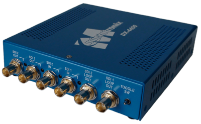
SDI VIDEO OVERLAY PRODUCTS
SDI VIDEO OVERLAY PRODUCTS
IP CORE AND FPGA PRODUCTS
IP CORE AND FPGA PRODUCTS
CONFIGURABLE PROCESSOR MODULES
CONFIGURABLE PROCESSOR MODULES
HSMC DAUGHTERCARDS
HSMC DAUGHTERCARDS
TECHNICAL SUPPORT CONTRACTS
TECHNICAL SUPPORT CONTRACTS
Tel:
+1 519 690-0091
Search
DESIGN SERVICES
NEWS
ABOUT US
CONTACT US
SITEMAP
TECHNICAL SUPPORT
REQUEST INFO
REQUEST EVALUATION
FAQs
TERMS & CONDITIONS
PRIVACY POLICY
© 2026
All Rights Reserved | Microtronix
Web Design by Strange Ideas
Share by: